Image Gallery
Gallery
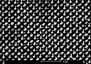
Photonic Crystal by Phase Mask Lithography

Media Details
Created 4/10/2007
SEM image of a photonic crystal structure fabricated using phase mask lithography. The XY grating periodicity of the phase mask (and the resulting pattern) is 1.57 microns. The grating was fabricated by backside exposure, through the substrate, near the edge of the sample, so some of the diffracted orders are missing from the interference pattern, giving an asymmetric unit cell.
Credits
- Matthew C. George , 3D Micro- and Nanosystems, Beckman Institute