Image of the Week Gallery
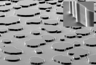
Plasma-Etched Silicon Wafer
Media Details
Created 4/19/2001 5:00:00 AM
This is a plasma-etched silicon wafer, produced from an image of natural sand. The silicon wafer was etched to a depth of 50 micrometers. The image was acquired on the ESEM in the Microscopy Suite.
Credits
- Cheema Chomsurin , Department of Civil and Environmental Engineering
Visualization Laboratory
Beckman Institute room 2203
405 North Mathews Avenue, Urbana, IL
(217) 300-0566