Image of the Week Gallery
Reactive Ion Etching Pattern
Media Details
Created 2/15/2005 6:00:00 AM
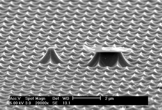
In this scanning electron micrograph we see an example of what may occur when anisotropic conditions for reactive ion etching are not achieved. The horizontal portions of the raised areas in this image are photoresist that was left floating above the silicon surface.
Credits
- Jeff Kim , 3D Micro- and Nanosystems, Beckman Institute
- John A. Rogers , 3D Micro- and Nanosystems, Beckman Institute
Visualization Laboratory
Beckman Institute room 2203
405 North Mathews Avenue, Urbana, IL
(217) 300-0566